找蓝光GaN-micro-LED仿真的文章带trap和不带trap的文章各五篇,嗯得多看点paper,之前的学习状态不对
这篇不赖ref:Designs of InGaN Micro‑LED Structure for Improving Quantum Efficiency at Low Current Density
用APSYS仿真的
几乎一模一样的参数,感动ing,文章主要对比了0.1A/cm2(1E-5)和200A/cm2(0.02A)处情况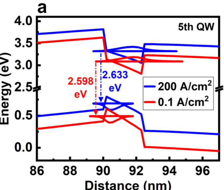
这个first level electron-hole wave function 有点意思
- 注入会减轻斯塔克效应,使得first-level“更正对”
- 因此,高注入电流会提高这个值
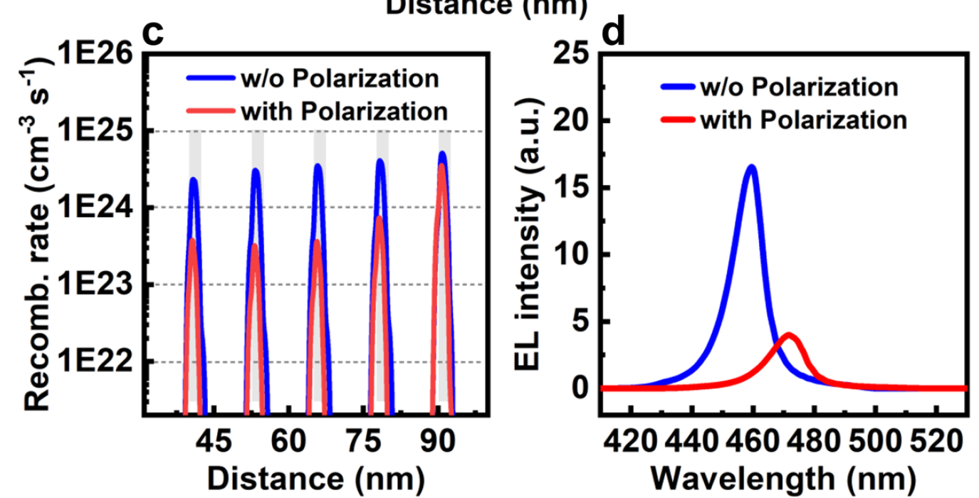
polarization会影响复合速率,具体体现在增加carrier集中的空间位置 - 从右图看出,靠近p级时受影响最小,说明这里的注入最高
GaN中,hole的浓度低一个量级,mobility低两个量级,这影响inject efficiency和radiative recombination rate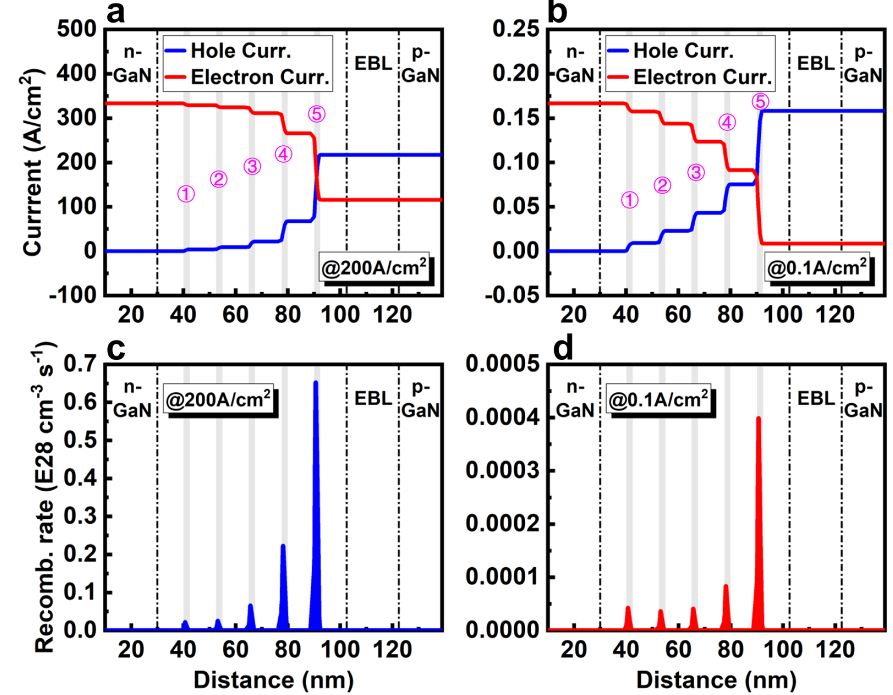
瞬态的电流密度可以超过总电流,没懂是怎么定义的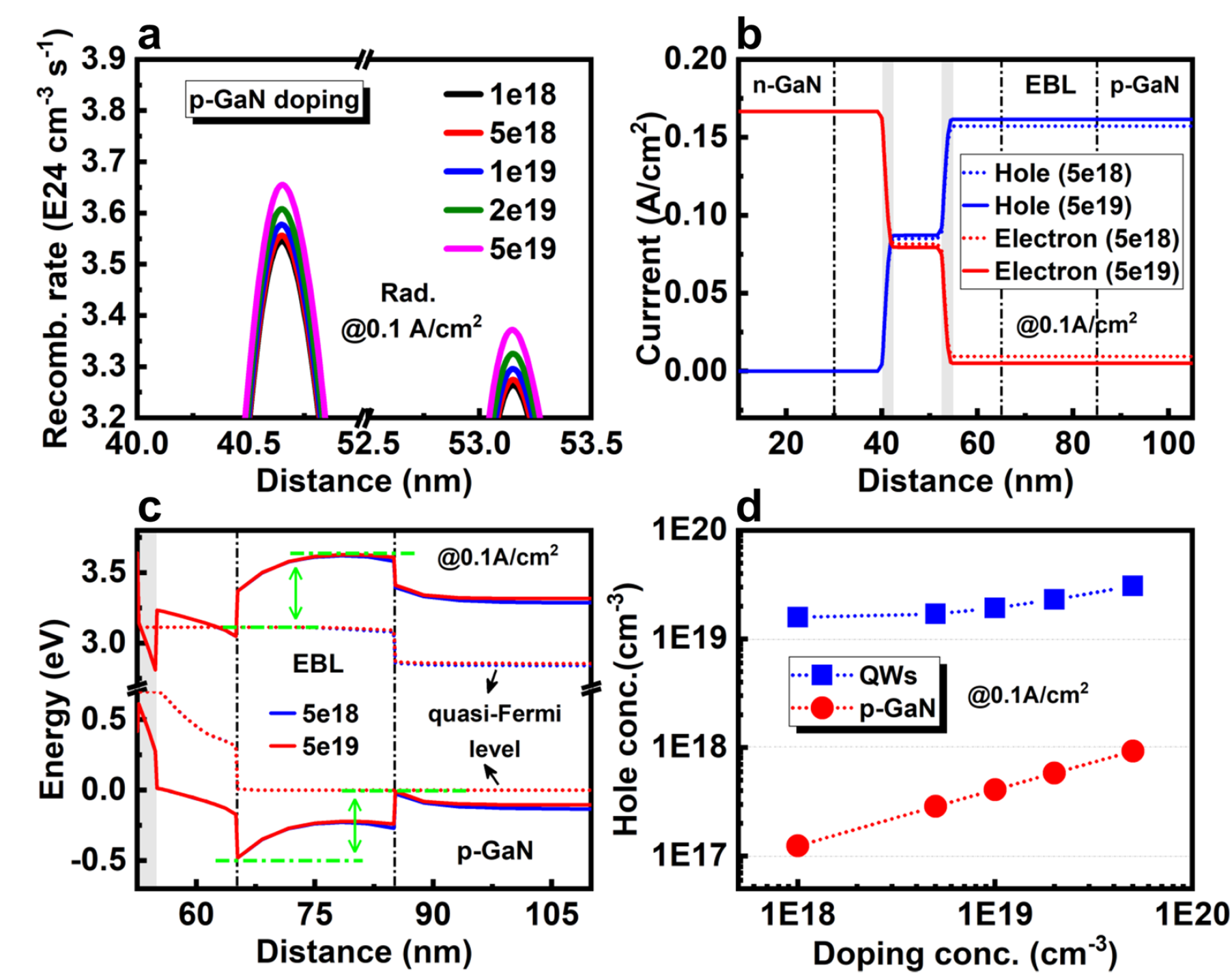
p-GaN对LED的影响很小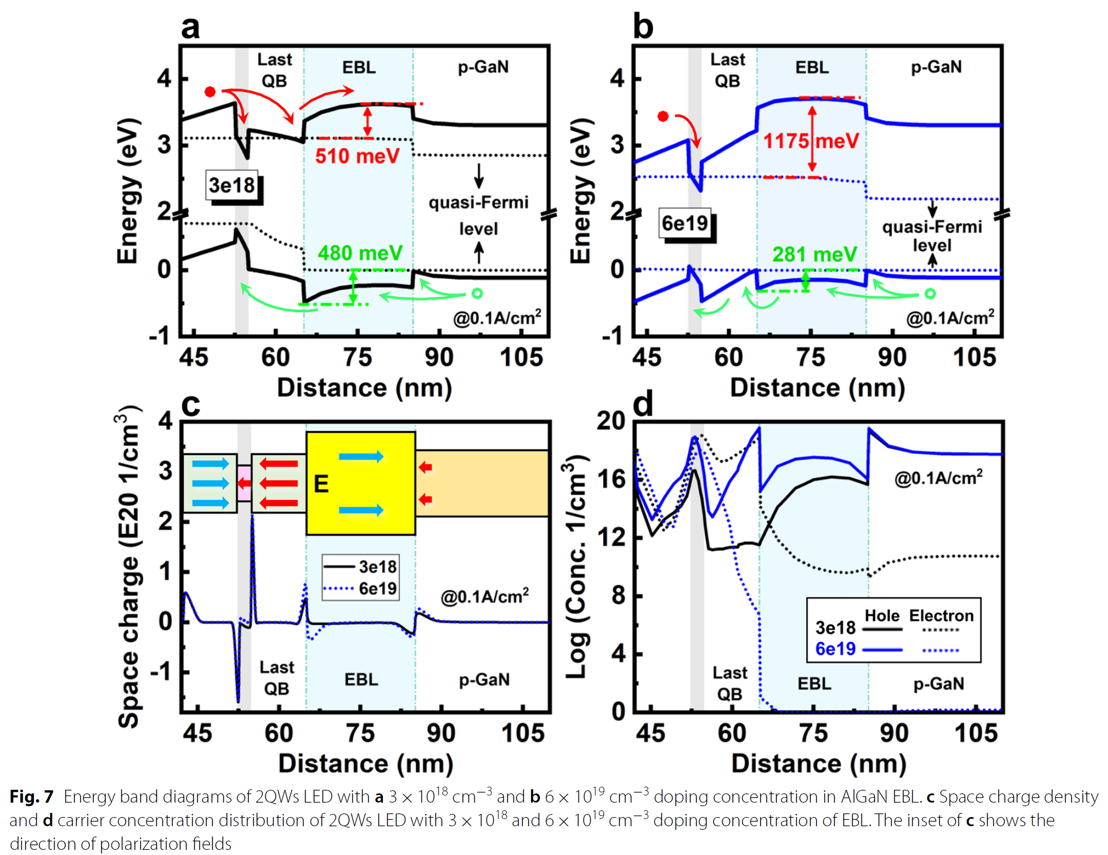
EBL中doping的影响就很大了,Aldoping和EBL都被fix了
- 最接近n端的electron会产生向下bending的电场,从而在EBL表面形成valley,如果该情况发生,blocking作用就失效了(见图d中EBL区域的高electron浓度)
- 同时,低concentration时也会增加hole inject的能垒
- 因此,增加EBL的pdoping是有利的,文中用的是“much higher”,因为Mg中的p的activation energy甚至更低
- 文中使用的6E19,drawback是形成了
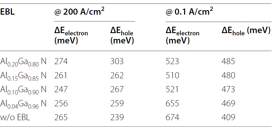
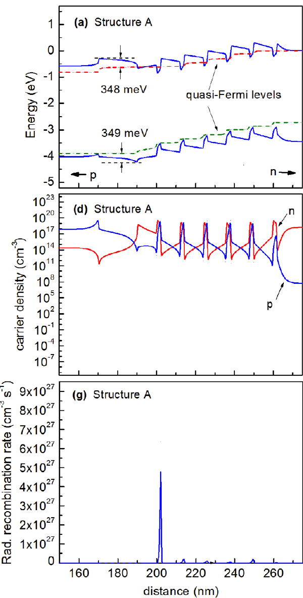
不同电流下的barrier hight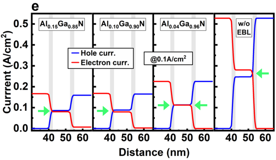
随着Al组分的减小,前面提到的不利效应出现减弱,观察到injection变得更优。文章的结论是去掉EBL会得到更好的injection。但是这么做应该会使漏电升高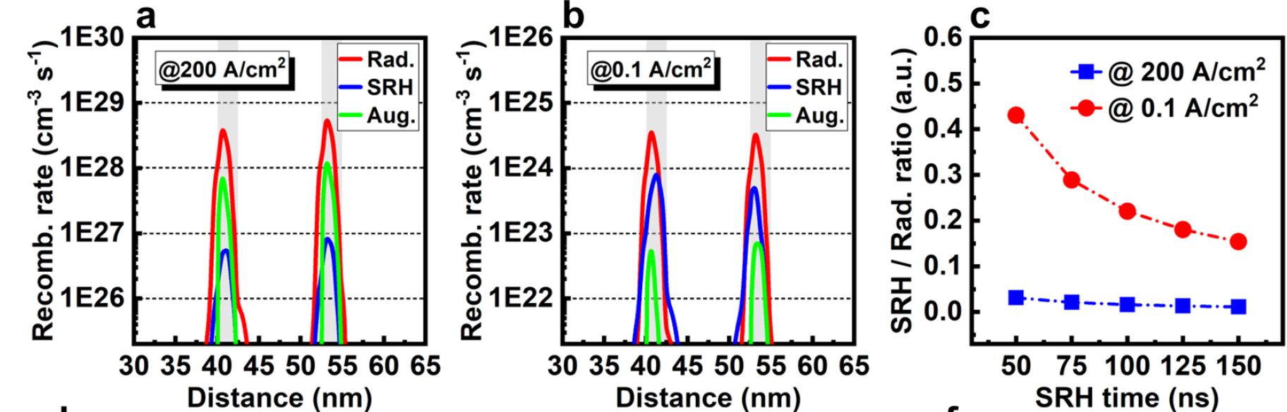
- 200A时的SRH占1E-2
- 0.1A时的auger可忽略,SRH comparable
文中提到Therefore, the effect of defect density can be estimated by simplychanging the SRH lifetime in the simulation.有点意思,回头去check一下handbook里面是怎么计算defect的
ref:Ultra-low-current driven InGaN blue micro light-emitting diodes for electrically efficient and self-heating relaxed microdisplay
这篇文章讲的是提升epi,抑制small size degradation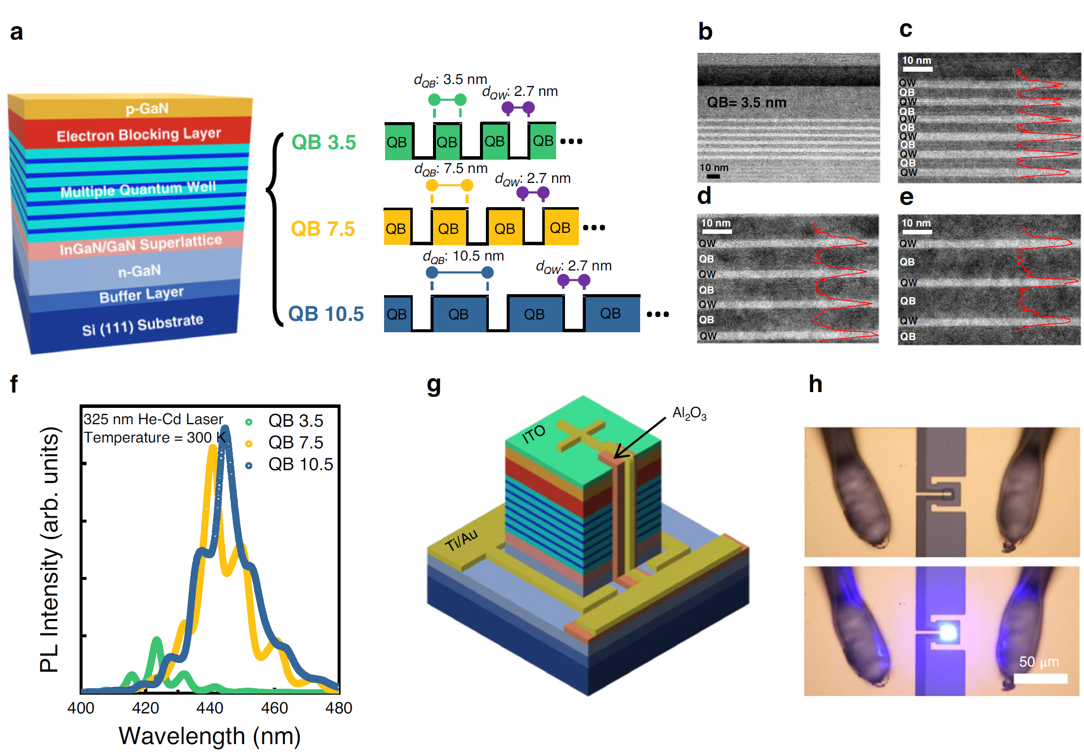
- 波长和构型都很契合
- 看左下的图,3.5nm的efficiency特别低,this could be attribute to the formation of the miniband near the interface.
用不同尺寸下的电流提取了surface和mesa的电流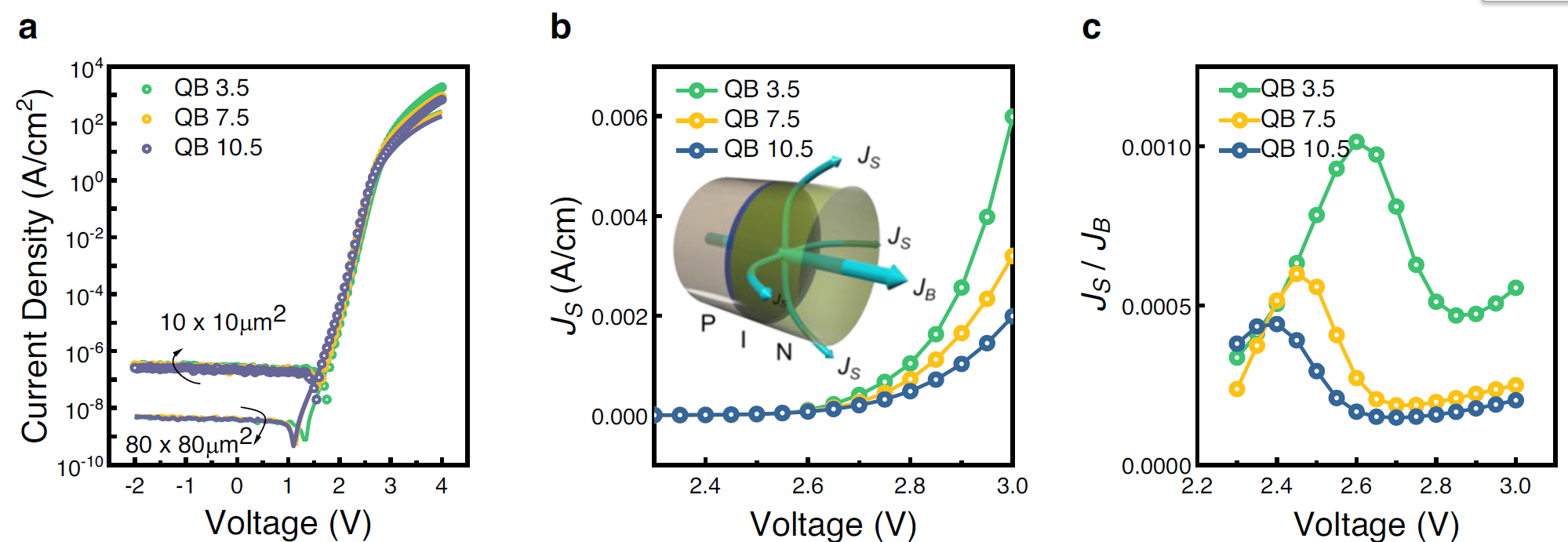
- 文章里还提到thicker QB could enhance EQE
- 同时thick QB 也提供了smaller Maximum EQE peak shift
ref:Analysis of nonradiative recombination mechanisms and their impacts on the device performance of InGaN/GaN light-emitting diodes
这篇文章还包括了In general, the ideality factors indicate the mechanisms of carrier transport and recombination: For instance, an ideality factor of one is caused by the band-to-band radiative recombination, an ideality factor of two is resulted from the Shockley–Read–Hole (SRH) recombination via defect levels, and an ideality factor greater than two is induced by the defect-assisted tunneling phenomenon.25,26 In other words, a decrease in ideality factor close to one from a value greater than one in Region 1 is caused by gradual predominance of the radiative recombination, while an increase in ideality factor in Region 2 is due to the series resistance.稍后再逐个看
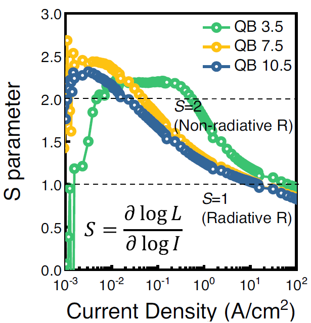
里面提到的这个S-parameter挺有意思的,但是需要测光,感觉本质和ideality factor无关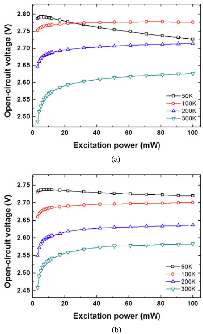
在低温下,SRH会收到抑制,while tuneling不受影响,因此50K时,A的pile up变得严重,为什么open circuit voltage减小没看懂。但B显示出与A不同的趋势
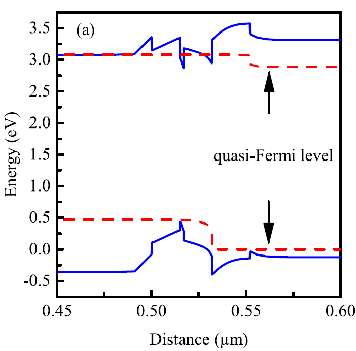
回到之前的文章,文章的仿真也是用SILVACO做的,以下的结果都是在电流0.1A时解的,调研一下是不是LED需要用电流密度仿真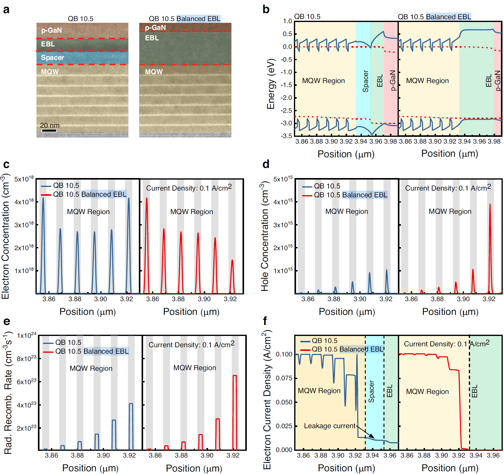
electron-hole concentration,racombination rate, electron current density, energy band
参数总结 - geometry 10*10um
- polarization 50%
这一项的意思是实际极化面电荷与理论电荷量之比 - band offset ratio 0.5:0.5
- surface recombination velocity 1E5cm/s 这一项很tricky
- The SRH recombination lifetime 100 ns
- radiative recombination 1 × 10⁻¹⁰ cm3/s
- Auger recombination coefficient 1 × 10⁻³¹ cm6/s
从supplement文件中可以找到0.1A注入时的banddiagram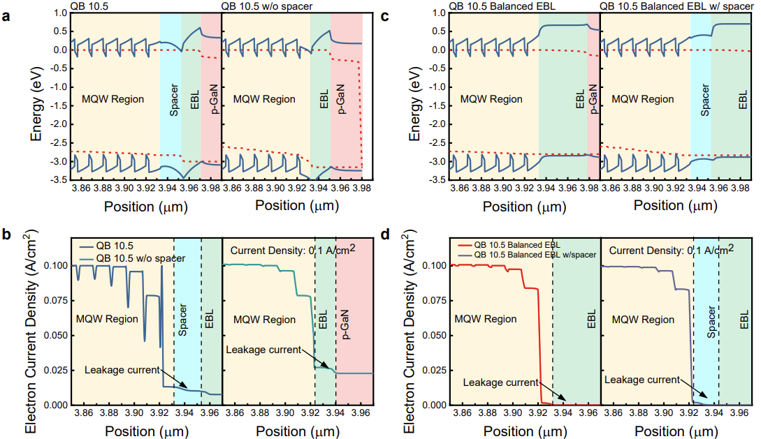
ref:Band parameters for nitrogen-containing semiconductors 材料parameter参考这篇,我勒个3000引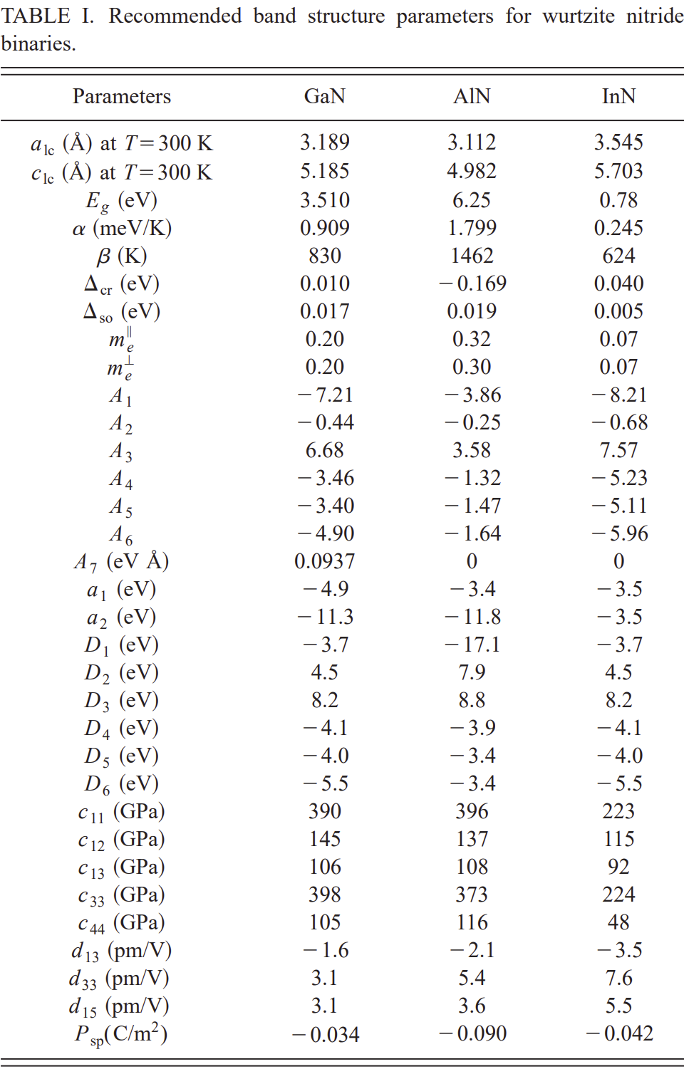
T-dependent bandgap
$$
E_g(T)=E_g(T=0)-\frac{\alpha T^2}{T+\beta},
$$
只给了electron的有效质量,因为空穴的质量是由下面公式决定的,能用上的也就Eg,电子质量,polarization
$$
E_g\left(A_{1-x} B_x\right)=(1-x) E_g(A)+x E_g(B)-x(1-x) C
$$
合金的bandgap如这个公式,需要知道C
InGaN:1.4eV
AlGaN:0.7eV
ref:A simulation study on the enhancement of the efficiency of GaN-based blue light-emitting diodes at low current density for micro-LED applications
用APSYS做的
band offset ratio:70:30(C:V)
- 设置了一个SRH internal loss
- The SRH recombination lifetime 100 ns
- radiative recombination 直接设置了0.78效率
- polarization也是50%
- Auger recombination coefficient 1 × 10⁻³¹ cm6/s
SRH,auger,polarization的值与上一篇相同,来看看bandoffset怎么设置
同样引自3000引这篇,应该是用导带顶距离和bandgap计算出的,我大概懂了,silvaco的默认设置来自03年这篇应该 - 0.5um nGAN
- 20nm Al0.15 1.2E18的p-doping
- 15nm ln0.1 barrier
- 2nm In0.225
- 发射波长450nm
1A/cm2注入时的bandeng
随后研究SQW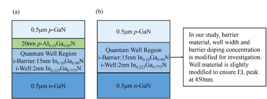
n-side doping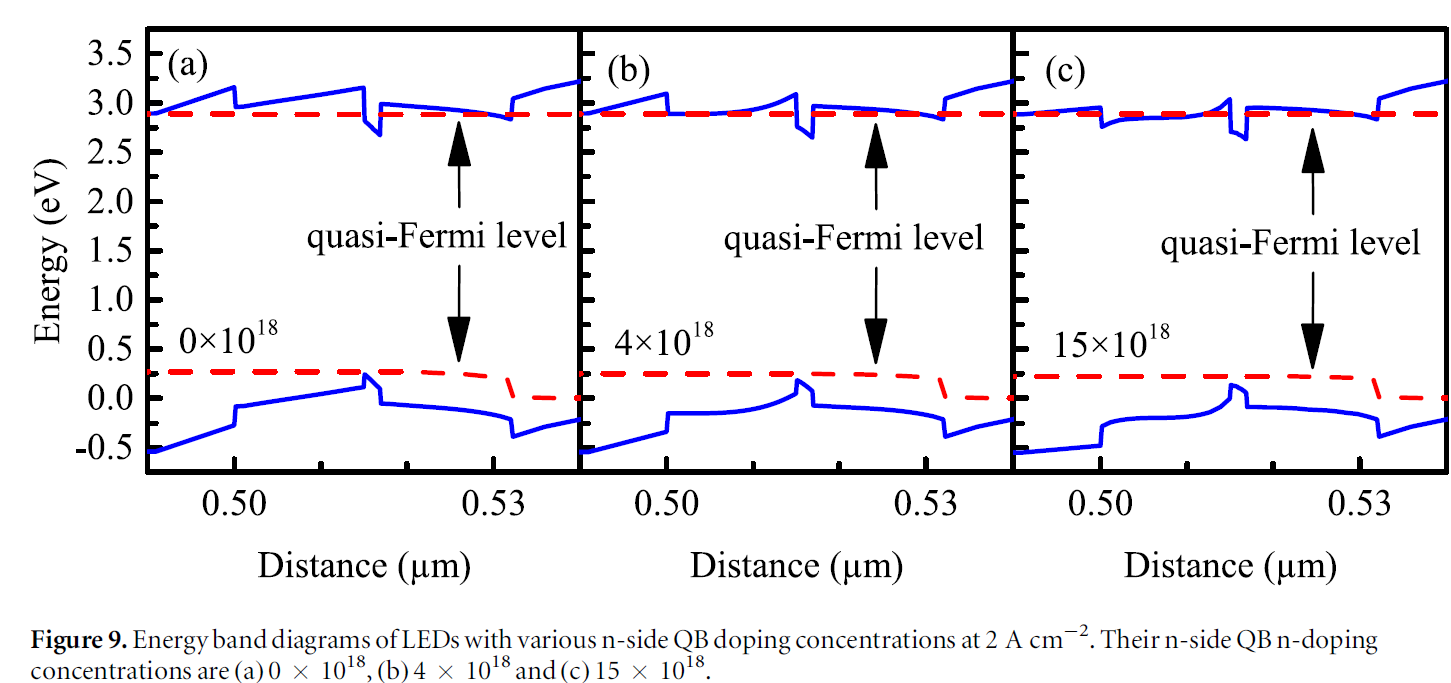
改变QBmaterial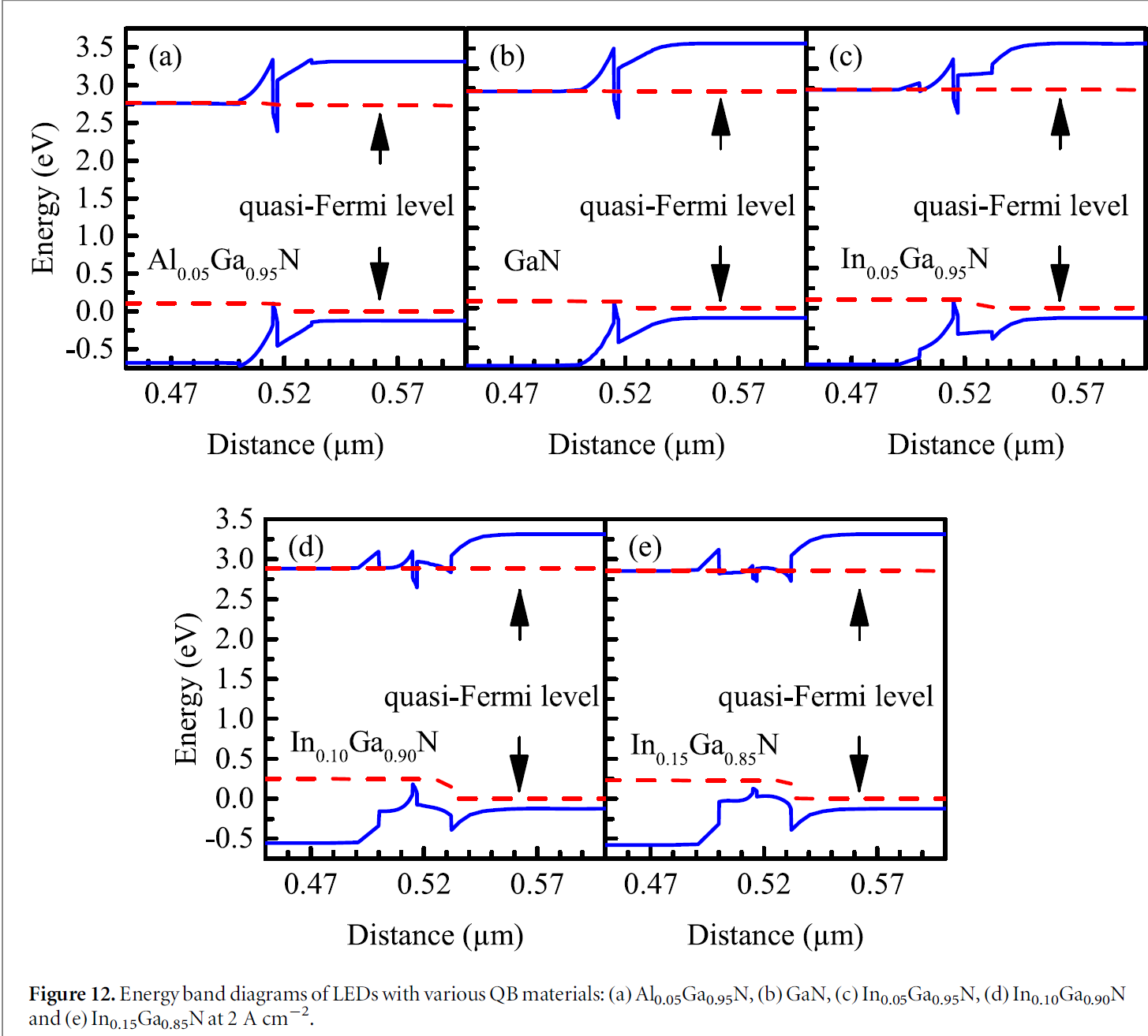
超大救星~
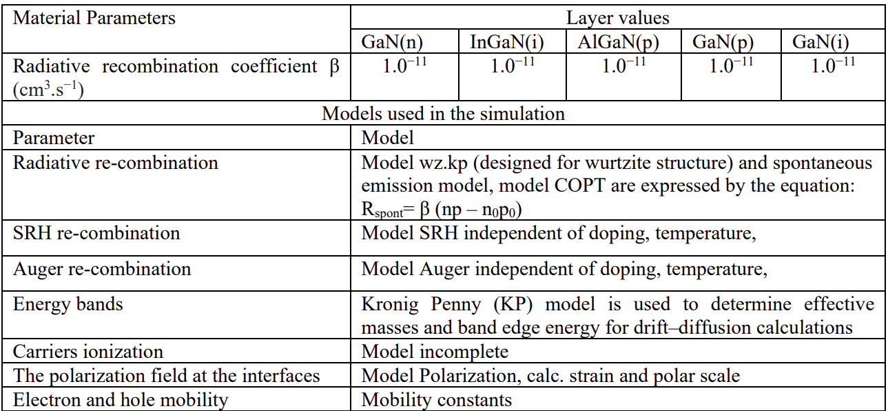
ref:Optimizing performance and energy consumption in GaN(n)/InxGa1-xN/GaN/AlGaN/GaN(p) light-emitting diodes by quantum-well number and mole fraction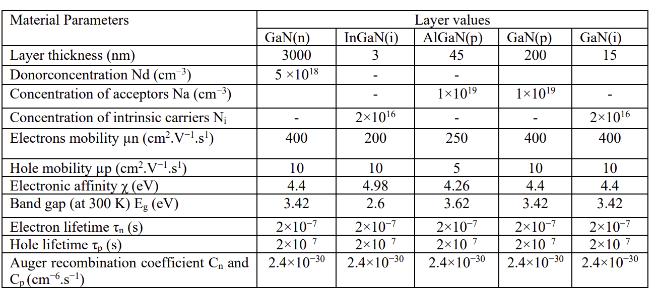
n-GaN: 3000nm
InGaN: 0.16; 3nm
QB intrinsic GaN: 15m (6 period in the active region)
EBL:Al0.15 dop 45nm
p-GaN: 200nm
其他方法:
- uniform doping
- block Newton method
- band offset使用atlas默认的0.7
使用的模型,我决定用这些参数作为后续模拟的setup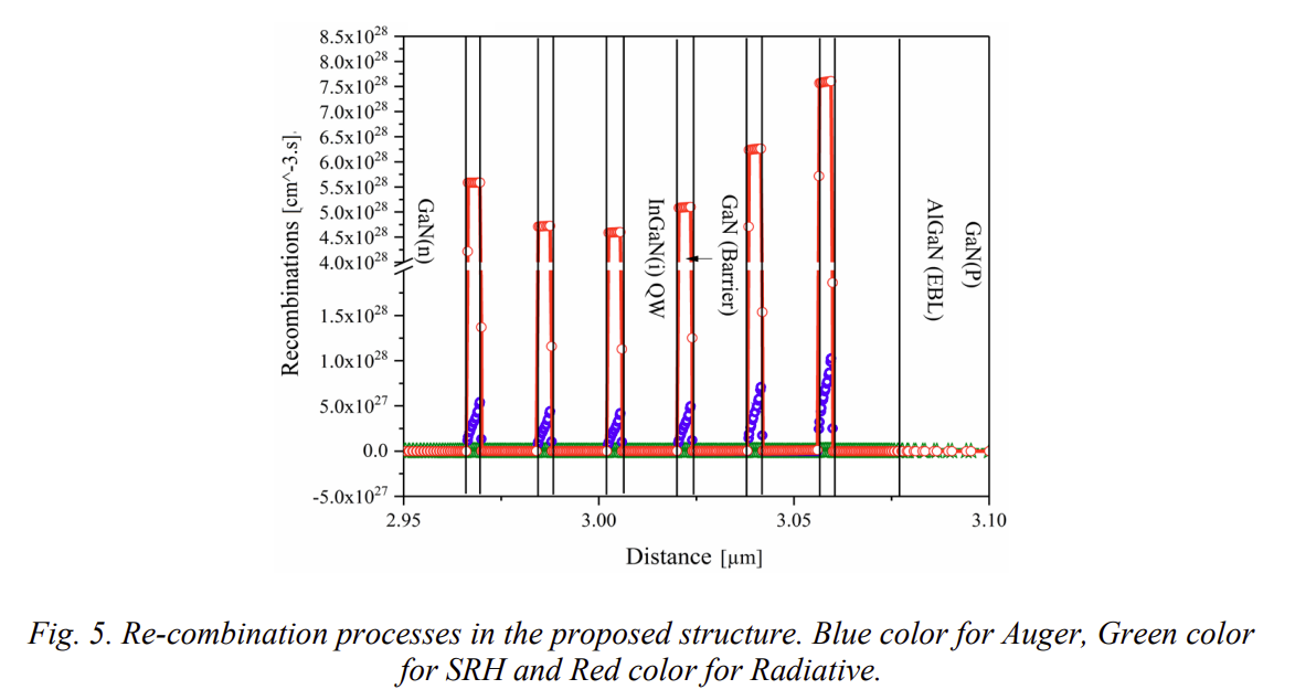
结论先不看了,这写得跟个实验报告似的……
用APSYS写的,用作来复现验证
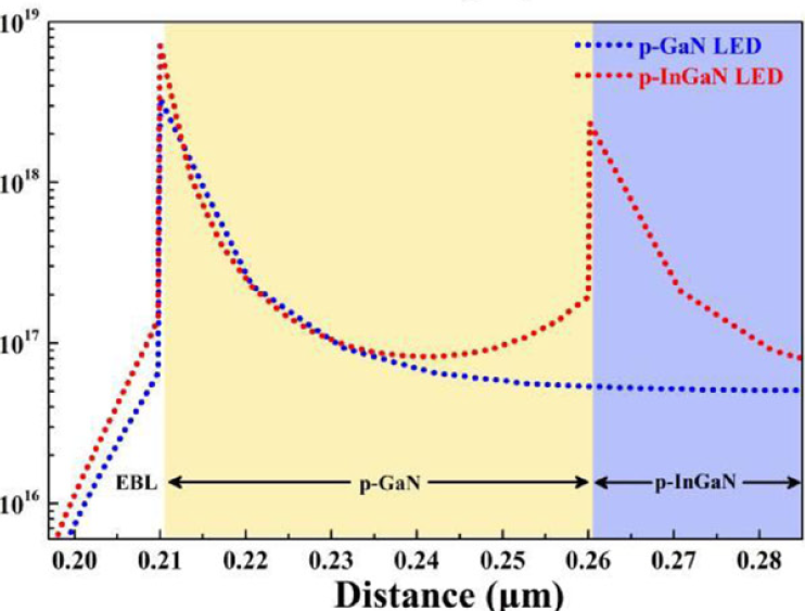
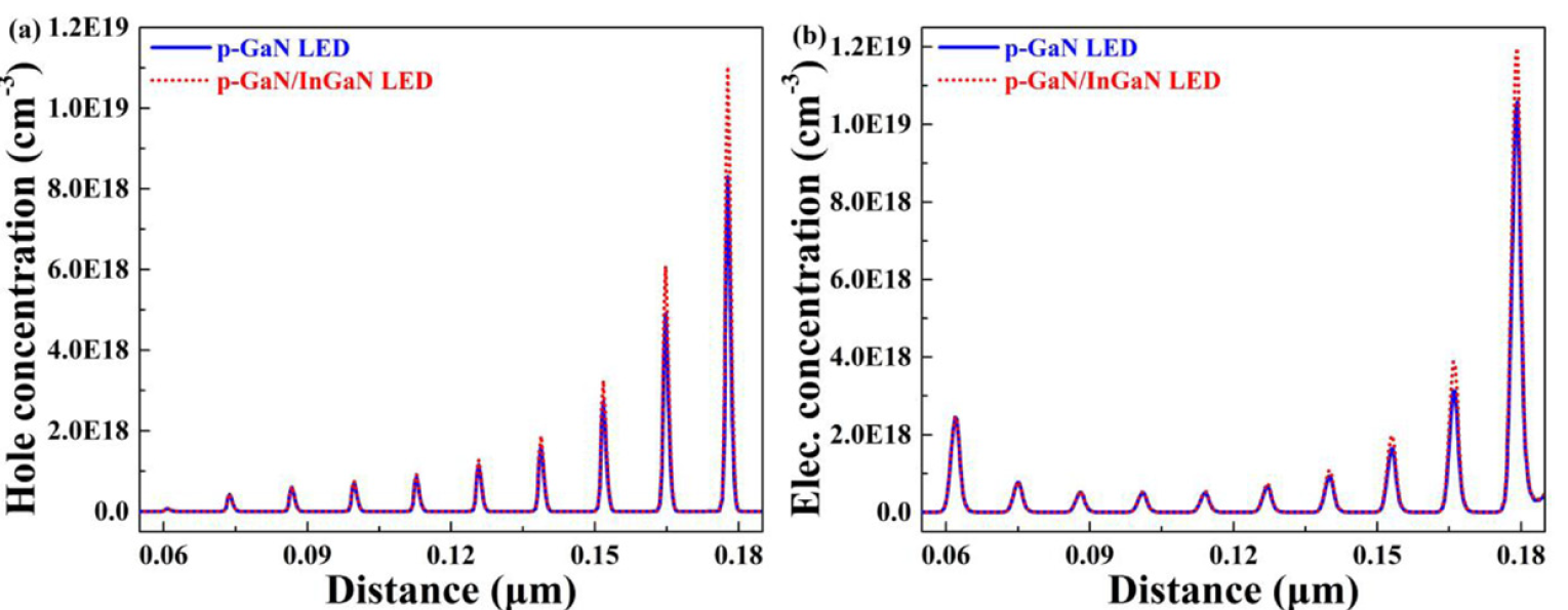
ref:A new structure of p-GaN/InGaN heterojunction to enhance hole injection for blue GaN-based LEDs
加了一层p-InGaN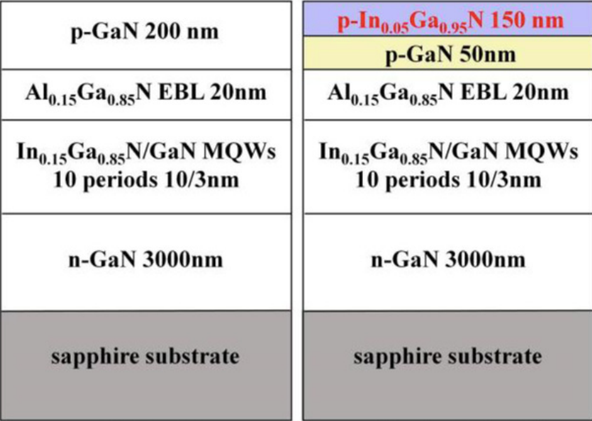
n-GaN:5E18
InGaN:0.15
EBL: Al=0.15; 7E17
p-GaN: 7E17
其他参数参照
ref:Sensitivity analysis of electron leakage in III-nitride light-emitting diodes
AlGaN:GaN=3.43;ALN=6.14,C=0.6
acceptor ionization : linearly from 170mV (GaN) to 470mV (AlGaN)
bandoffset = 0.6
模拟条件:100A/cm2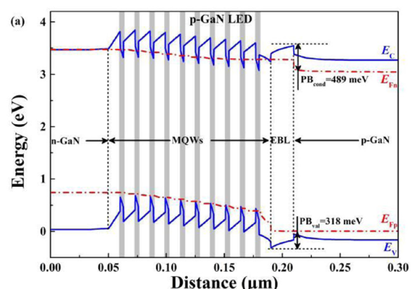
ref:Efficiency enhancement of InGaN/GaN light-emitting diodes with pin-doped GaN quantum barrier主要研究QB的影响,使用1D-DDCC,是一款轻量级软件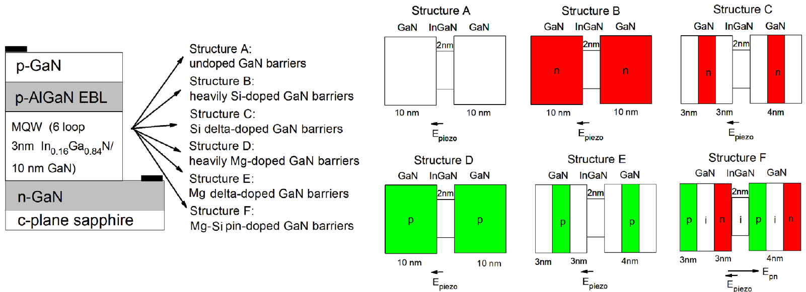
我们复现的重点应该是A构型(1E16)
- n-GaN: 5E18,2000nm
- EBL:AL0.15, 1E19,20nm
- p-GaN:2E19
其他信息: - Si ionization energy: 20mV
- acceptor ionization : linearly from 170mV (GaN) to 470mV (AlGaN)
- polarization: 0.5
- The SRH recombination lifetime 100 ns
- radiative recombination 2 × 10⁻¹¹ cm3/s
- Auger recombination coefficient 1 × 10⁻³¹ cm6/s
仿真电流密度:100A/cm2