从atlas入手学一下electro-thermal modeling,在网上找了找资料,发现在有gpt的辅助下,分析atlas官方提供的例子应该是最舒服的,毕竟它们的例子是可收敛的hhhh,阶段目标是学习热仿真的案例,然后复现sic JEFT 的热场分布(用silvaco的)
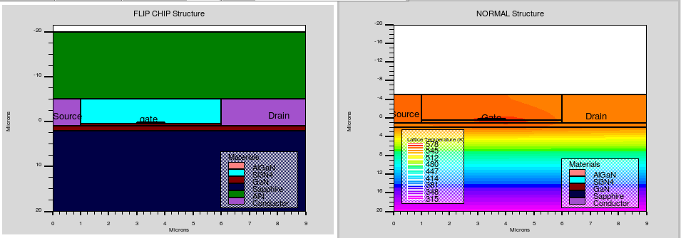
1
2
3
4
5
6
7
8
9
10
11
12
13
14
15
16
17
18
19
20
21
22
23
24
25
26
27
28
29
30
31
32
33
34
35
36
37
38
39
40
41
42
43
44
45
46
47
48
49
50
51
52
53
54
55
56
57
58
59
60
61
62
63
64
65
66
67
68
69
70
71
72
73
74
75
76
77
78
79
80
81
go atlas simflags="-80" #改变内置的参数,使用电热耦合时必加 mesh width=100 ^diag.flip #目的不明,疑似y轴翻转 region num=1 x.min=0.5 x.max=8.5 y.max=0.5267 mat=AlGaN x.comp=0.25 region num=2 x.min=0.0 x.max=9.0 y.min=-5 y.max=0.5 mat=nitride insulator region num=3 x.min=0.5 x.max=8.5 y.min=0.5267 y.max=1 mat=GaN donors=1e15 substrate region num=4 x.min=0.0 x.max=9.0 y.min=1.0 y.max=2.0 mat=GaN region num=5 x.min=0.0 x.max=9.0 y.min=2.0 y.max=20.0 mat=sapphire insulator region num=6 x.min=0.0 x.max=9.0 y.min=-20 y.max=-5 mat=AlN elec num=1 name=source x.min=0 x.max=1 y.min=-5 y.max=1 elec num=2 name=drain x.min=6 x.max=9 y.min=-5 y.max=1 elec num=3 name=gate x.min=3 x.max=4 y.min=0.2 y.max=0.5 elec num=4 substrate #注意这段代码,将substrate设置在GaN,蓝宝石设置为电绝缘,主要起导热作用 #为什么将接触是一个二维区域,因为文章中的器件是肖特基接触,肖特基接触的场的影响被限制在这个区域 models k.p print srh model lat.temp mobility FMCT.N Gansat.N #热学模型,K模型,GaN中的mobility行为 model polarization calc.strain polar.scale=0.75 model region=1 pch.elec interface neutralize x.min=3 x.max=4 y.min=0.48 y.max=0.52 #极化,极化其实分为三步,第一步启用polarization,这一步计算出的极化电场和电荷,实际上是直接线性叠加在原来电场上的,准确性有限 - 使用pch指令,在AlGaN中启用,将极化现象加入泊松方程求解中增加精度 - 对于p-GaN而言,其下方的trap和surface states可以部分补偿2DEG的电场,从而一定程度屏蔽对Gate的电势,因此,在gate-AlGaN界面创建一个电中性区域有助于收敛 thermcontact num=1 y.min=-20 y.max=-20 ext.temp=300 alpha=5000 #这个给出的就是热对流边界条件,不过5000稍微有点小了,我看的简化建模substrateboundary是404嘻嘻 solve previous solve vdrain=0.01 solve vdrain=0.1 solve vdrain=1 solve vstep=1 name=drain vfinal=5 solve name=gate vfinal=-10 vstep=-0.5 log outf=ganfetex14_0.log solve name=gate vfinal=1 vstep=0.25 log off #电压step #在atlas中使用全局变量的方法 set vstart = 0 set vstop = 15 set vinc = .5 solve init solve vgate=-3 log outf=ganfetex14_1.log solve name=drain vdrain=$vstart vfinal=$vstop vstep=$vinc log off #在atlas中使用全局变量的方法 log outf=ganfetex14_5.log master gains s.params inport=gate outport=drain solve ac freq=10 fstep=10 mult.f nfstep=7 solve ac freq=1e9 solve ac freq=2e9 fstep=2e9 nfstep=3 solve ac freq=1e10 fstep=5e9 nfstep=8 log off #交流下的增益等信息,稍后补充 solve name=gate vfinal=-10 vstep=-0.5 LOG outf=ganfetex14_13.log solve Vgate=0 ramptime=1e-8 dt=5e-10 tstop=1e-8 solve dt=1e-9 tstop=1e-7 solve dt=1e-8 tstop=1e-6 solve dt=1e-7 tstop=1e-5 solve dt=1e-6 tstop=1e-4 #先到-10,然后猛地打开(到零) #第一行规定了ramptime(也就是pulse) #随后是指数级的采样点,由密到疏观察整个过程
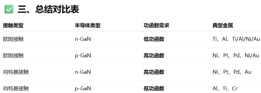
插播复习一下欧姆接触和肖特基接触
不管是p还是n型材料的接触,载流子都是从金属流向半导体,载流子种类不同
金属没有禁带,同时含有丰富的自由电子,可以视为一个电子源
欧姆接触阻挡载流子流动的方向,同时要求能垒尽可能的窄,实现隧穿
肖特基接触要求从金属流出的时候不阻挡(那么反向就一定会阻挡)
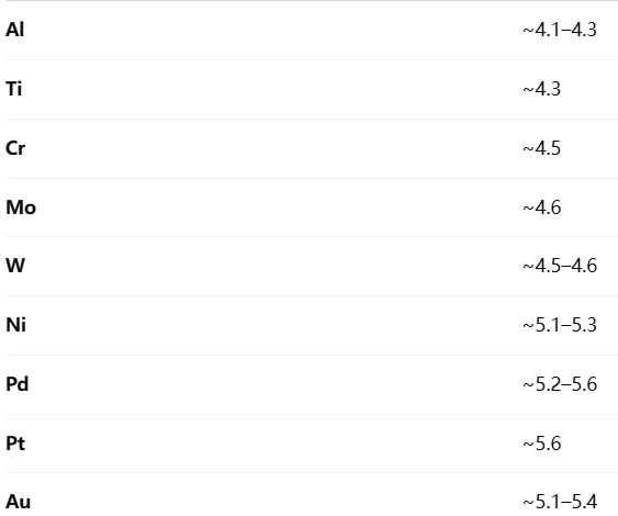
然后是判断金属电子亲合能于半导体的相对大小,电子亲合能是费米能级到真空能级所需的能量,接触时假设真空能级是对齐的
当金属的费米能级低时(高功函数),接触时电子从半导体流向金属。从而在界面堆积形成正电荷
当金属的费米能级高时(低功函数),接触时电子从金属流向半导体。从而在界面堆积形成负电荷
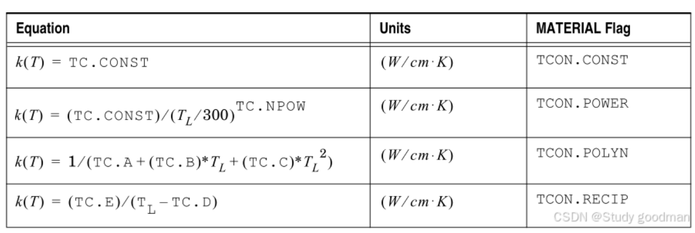
1 material mat=Diamond TCON.POWER TC.NPOW=2 TC.CONST=1.4 #使用TCON.POWER模式,设置TC.NPOW,TC.CONST参数
1
2
3
4
5
6
7
8
9
10
11
12
13
14
首先使用了图形化编辑器go devedit,回头看看deckbuild里面能用吗 material material=4H-SiC permitti=9.66 eg300=2.99 \ edb=0.1 gcb=2 eab=0.2 gvb=4 \ nsrhn=3e17 nsrhp=3e17 taun0=5e-10 taup0=1e-10 \ tc.a=100 首先定义了和能带相关参数 mobility material=4H-SiC vsatn=2e7 vsatp=2e7 betan=2 betap=2 \ mu1n.caug=10 mu2n.caug=410 ncritn.caug=13e17 \ deltan.caug=0.6 gamman.caug=0.0 \ alphan.caug=-3 betan.caug=-3 \ mu1p.caug=20 mu2p.caug=95 ncritp.caug=1e19 \ deltap.caug=0.5 gammap.caug=0.0 \ alphap.caug=-3 betap.caug=-3 然后是和mobility相关的参数
$$
1
2
3
4
5
6
7
8
9
10
11
12
13
14
15
16
17
mobility material=4H-SiC vsatn=2e7 vsatp=2e7 betan=2 betap=2 \ mu1n.caug=10 mu2n.caug=410 ncritn.caug=13e17 \ deltan.caug=0.6 gamman.caug=0.0 \ alphan.caug=-3 betan.caug=-3 \ mu1p.caug=20 mu2p.caug=95 ncritp.caug=1e19 \ deltap.caug=0.5 gammap.caug=0.0 \ alphap.caug=-3 betap.caug=-3 # # Now define mobility in plane <1000> # mobility material=4H-SiC n.angle=90.0 p.angle=90.0 vsatn=2e7 vsatp=2e7 \ betan=2 betap=2 mu1n.caug=5 mu2n.caug=80 ncritn.caug=13e17 \ deltan.caug=0.6 gamman.caug=0.0 \ alphan.caug=-3 betan.caug=-3 \ mu1p.caug=2.5 mu2p.caug=20 ncritp.caug=1e19 \ deltap.caug=0.5 gammap.caug=0.0 \ alphap.caug=-3 betap.caug=-3
通过改变n.angle=90.0 p.angle=90.0来实现各向异性的仿真
HyFET同时包含了横向和纵向的电流通路,各向异性的mobility模拟很重要!
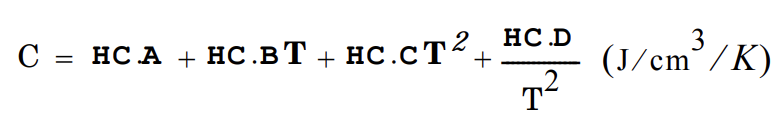
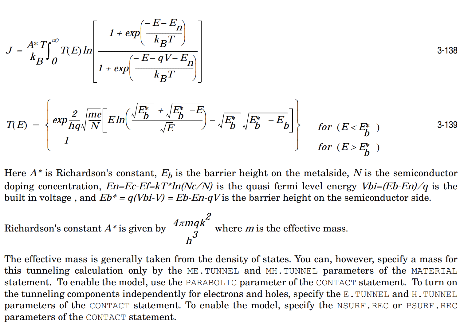
1
2
3
4
5
6
material material=4H-SiC affinity=3.13 \ TCON.POWER TC.CONST=3.70 TC.NPOW=1.25 \ HC.STD HC.A=1.79 HC.B=0.00097 HC.C=0.0 HC.D=0.0 \ taun0=5.0e-10 taup0=1.0e-10 ARichN=146 \ me.tunnel=0.3 mh.tunnel=0.3 d.tunnel=1.0e-6
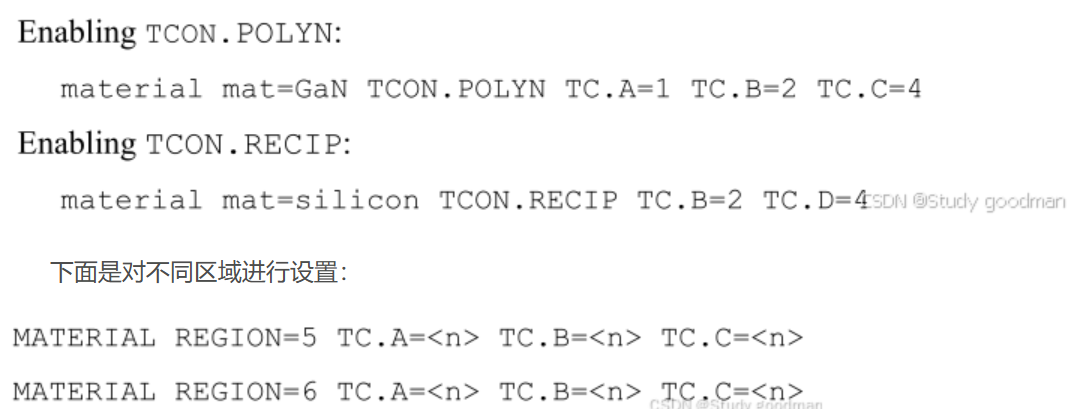
TCON系列前面提到过,
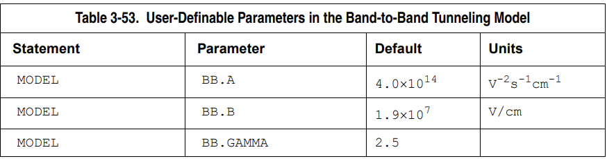
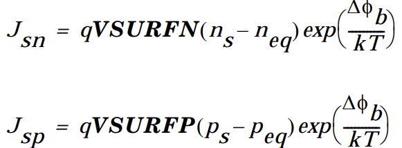
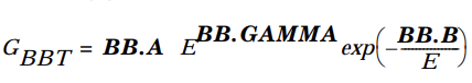
1
2
3
4
5
6
7
8
9
contact name=anode workfunction=4.7 surf.rec barrier \ me.tunnel=0.3 mh.tunnel=0.3 surf.rec barrier指肖特基结的表面复合,不默认开启 models Temp=300 BGN Analytic SRH fldmob Auger UST print \ BBT.STD bb.a=8e7 bb.b=9e6 bb.gamma=2.6 \ incomplete inc.ion fldmob,电场-迁移率依赖 bb系列是band to band transition的参数
1
2
impact aniso e.side be0001=2.18e7 bh0001=2.03e7 ae0001=3.82e8 ah0001=3.10e8 简化的impact ionization模型,参数没找到
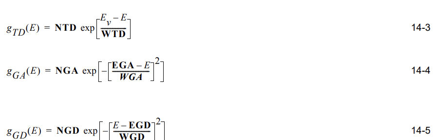
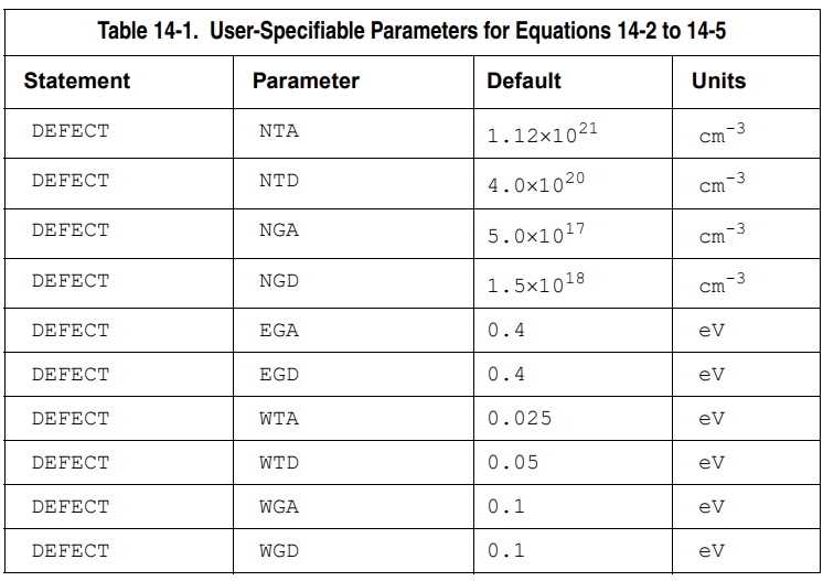
1
2
3
4
5
6
7
8
9
go atlas simflags="-160" doping p.type gaussian concentration=3.0e19 charac=0.2 peak=0.25 \ x.min=7.99 x.max=9.51 高斯参杂 intdefects tfile=sicex07.dat numa=24 numd=24 continuous \ ega=0.805 egd=0.805 nga=2e11 ngd=2e11 wga=1 wgd=1 \ nta=1e14 ntd=1e14 wta=0.1 wtd=0.1 关于defects的设置,来补课一下TAT
Density of States Model
Demo中使用的continuous语句的原文如下:
1 
这个地方好像重复声明了,经过画图检验,continuous中文件包含的gE就是下面两行参数的计算结果;下两行参数也复合atlas manual里的格式
1 
method climit=1e-20 itlimit=50
mesh infile=ledex03.str scale.x=100
1 2 3   仿真主要研究横向电流
region num=2 modify material=InGaN qwell led well.ny=40
1 2 3 4 5 6 7 8 9 10 11 12 13 14 15 16 17  比较关键的是解一维sch方程,求解时需要确定一个NY,对于每个segmentation 求解一维sch方程,解出来后值映射到mesh上。kp方程是假设晶体为一维周期性势场的情况下解出电子,空穴有效质量/禁带宽度的方法 得到有效质量后就可以根据polarization求解drift-diffuse方程惹 WELL.CNBS and WELL.VNBS是求解sch方程的最大能带数  求解流程为: - 泊松方程给出电荷分布,根据势阱宽度得到特征值E,带入sch求得波函数 - 波函数的平方得到概率,费米狄拉克分布得到新的电荷密度 - 得到新的电荷分布后,根据泊松方程更新势场 - 交替求解直至收敛 接下来总结MQW需要定义的参数 - YMIN和YMAX,大于MQW区域 (NWELL) - NBS限制最大能带数 - 设置其他参数 接下来学学probe
probe name=”Radiative” radiative integrate x.min=0 x.max=350 y.min=0.6 y.max=0.603
1
2
再看看另一个 
material material=GaN taun0=1e-9 taup0=1e-9 copt=1.1e-8
material well.gamma0=30e-3
region num=3 material=InGaN y.min=0.604 y.max=0.611 x.comp=0.20 name=well
material well.taup=1e-12 well.taun=1e-12#单独设置发射时间
models name=well qwell led
 impact aniso e.side be0001=2.18e7 bh0001=2.03e7 ae0001=3.82e8 ah0001=3.10e8