任务已经明晰
- literature review
- 找到商用片的参数并仿真
找到商用片,分开复现
2d仿真热源模型,然后跑package - 同步学习comsol-问一下
ref:Stacked Strongly Coupled GaN/SiC Cascode Device With Fast Switching and Reclaimed Strong dv/dt Control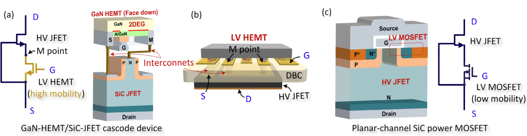
cascode的截面图,文中用SiC LVmosfet作比较,cascode的优点在于,channel的mobility高,变为常开式的代价小
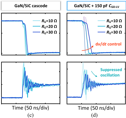
这篇文章的核心是dv/dt;low interconnection inductance,increased capative gate-to-drain coupling
1.2kV/68-m+40/3m
380um direct-bonding-copper (DBC)
According to the simulation results based on Q3D software, the parasitic inductance Lp is reduced to less than 80 pH
A double pulse test (DPT)
了解一下双脉冲测试DPT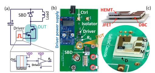
目的是模拟实际的开关过程,反偏的SBD模拟了GS短接情况下器件的反偏电阻,Load模拟了开关开启时的电感,为了实现minimum的开关器件,实际上需要减少从D端出发的电容DG+DS。GaN HEMT 的GD天然的小,优化的方向是DS
什么是tunable dv/dt? dv/dt会引起电磁波,通过modulate dv/dt(改变Rs)来限制发射的电磁干扰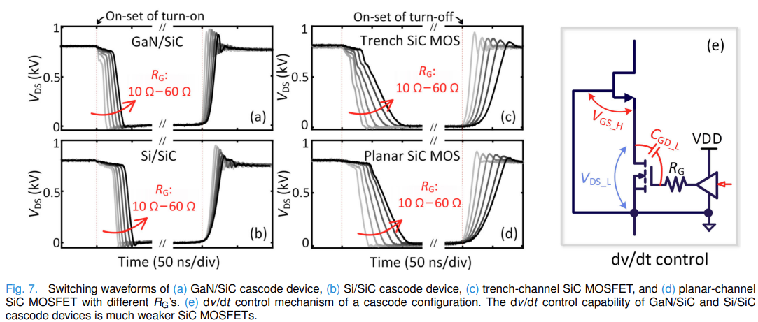
GaN/SiC 的controlability比Si/SiC更好,但是比Trench和planer SiC差
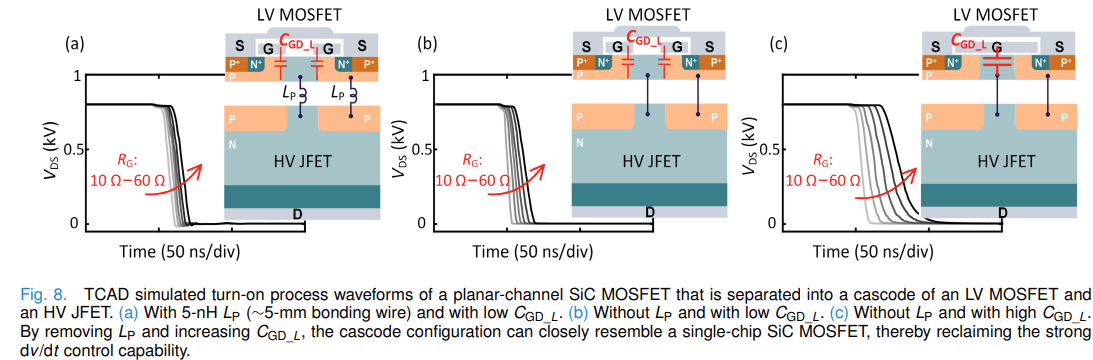
Indeed, the dv/dt of a cascode configuration is ultimately controlled by the gate bias of the HV device (VGS_H) [Fig. 7(e)], which is coupled to VDS of the LV device (VDS_L) through LP. VDS_L, in turn, is controlled by the gate driver circuit of the control device through the drain–gate coupling capacitor CGD_L. Such a two-step indirect dv/dt control mechanism of the cascode configuration requires strong coupling within both steps to enable strong dv/dt control for the cascode device.
改变整个器件通过改变H-VDS
H-Vds通过H-Vgs控制H的阻值
H-Vgs通过L-Vds控制
L-Vds通过gate电压控制
当gate从0->1时,通过CGD开启沟道,VDS迅速下降,L-VD的电压下降(via VGD),同时LVS的和HVS共同连接到G。L-VD从高到低的变化时,通过L的电流剧烈增加,从Hs到Ld的电流增加,while另一条负责HG和LS接地的连接依然没有电流通过,此时形成互感,阻碍电流的变化电感:复习一下,通电直导线周围会产生磁场(电流元产生磁场平方反比积分出来),闭合回路的磁通变化产生感应电动势
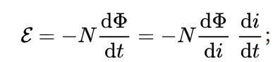
定义V=L*di/dt;L=dfai/di
实际情况下的导线电感计算比较复杂,总之越短电感越小
回到文章的结论:
- 考虑Lp比不考虑Lp的di/dt controlability 更差
- Gate电容越大时controability 更好,这解释了为什么SiC的controlability更好
- commercial Si/SiC cascode用bonding wires,因此即使Cgd大也失去了controability
- 比起没有interconnection的Single mosfet 依然差得远
因此,想要提高controllability, 直接的办法是 增加CGD_L,这是否会影响overall CGD呢,并不,因为在正向饱和以后,JFET出现pinch off, while VL-DS稳定在VTH,因此,CGD会被JFET的depletion电容主导,这个电容是很小的。通过并联电容,实现了很强的controllability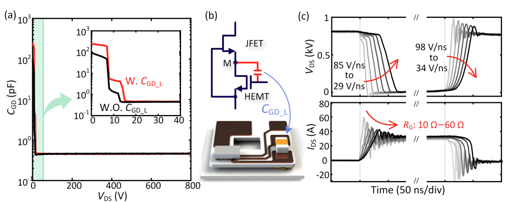
电感在瞬态时能主导电压,而整体的分压ir=L*di/dt 是一阶微分方程,因此会出现正弦解,电阻越大震荡被抑制得越厉害,因此有必要证明过冲电流不会影响GaN的正常工作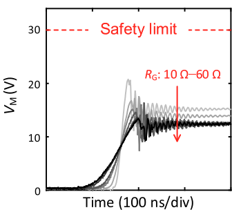
ref:Unlocking the Full Potential of GaN/SiC Cascode Device With 3D Co-Packaging and Enhanced dv/dt Control Capability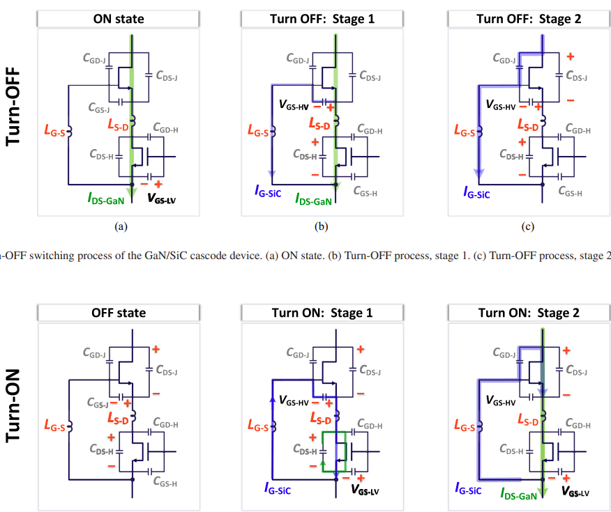
很简单,开态就是VGS-H逐渐充电的过程(JFET关断),关闭就是VGS-H放电